Unpatterned wafer particles inspection
Particles detection on transparent, classic, and exotic substrates

Ready to use particles inspection systems for transparent and opaque substrates

Eumetrys provides wafer surface equipment for transparent and opaque substrates (SiC, GaN, Crystal, Sapphire, Si…). YPI products line has the advantage to have a low cost of ownership while being adaptable to the customer’s need. For example, it allows process and particles contamination control with measures on EPI wafers or with SiC films.

To answer all the needs of the semiconductor industry and to share our support experience, Eumetrys is associated with YGK and enriches its offer with efficient and versatile products. This Japanese company is present in the semiconductor industry for more than 20 years and its primary objective is to design high quality particles contamination analysis equipment. This partnership combines YGK’s products performance with the efficiency and the responsiveness of Eumetrys’ experts.

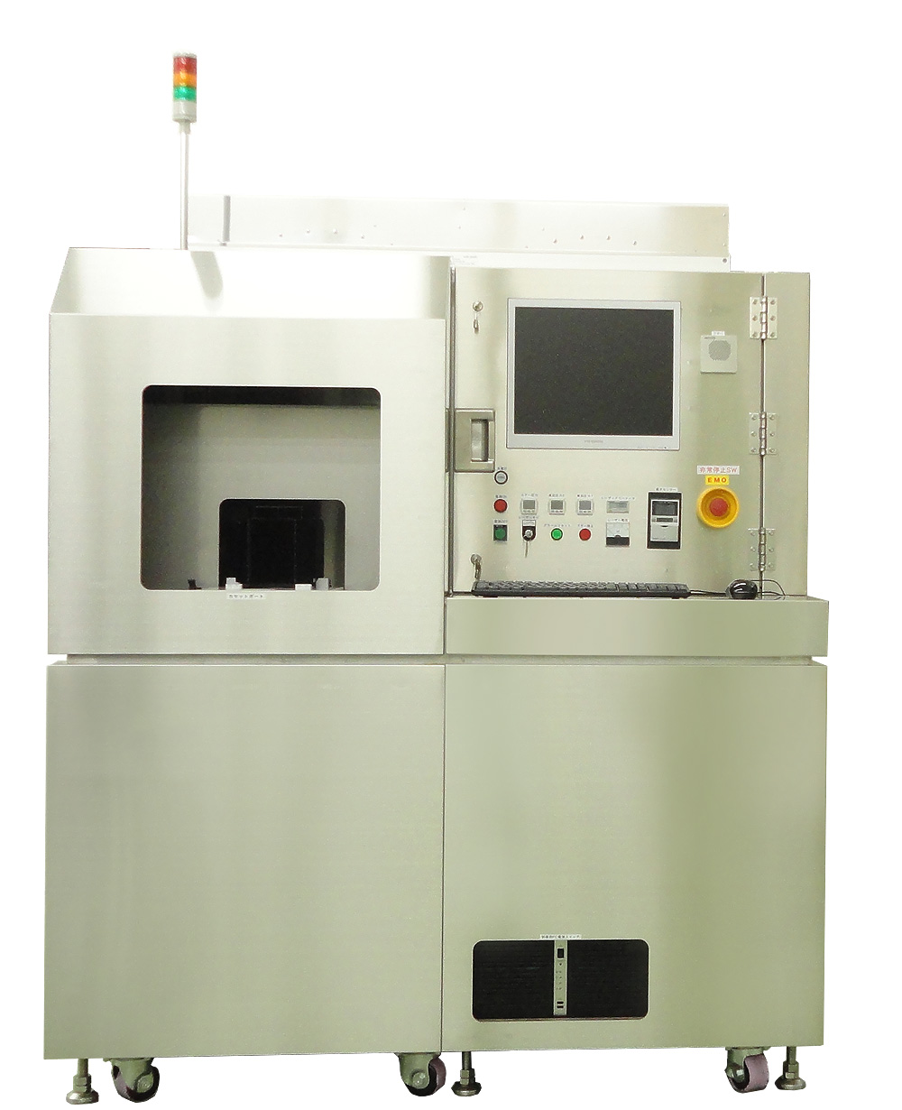
Transparent substrates benefit of an innovative technology embedded on the YPI-MX-DC equipment. Inspect particles contamination of your SiC and GaN wafers from 2 inches to 8 inches. Fully customizable and affordable, this tool meets all the expectations in terms of control of classic, translucent, transparent wafers or with thin layers. Learn more about this product by clicking here.

YPI-MX equipment is intended to silicon and compound semiconductor industries. It allows to control contamination of a great variety of substrates such as Si, Crystal, Sapphire, LiNb03 or even LiTa03 on every wafer size up to 8 inches. Discover in detail every capability of this tool by clicking here.

YPI-MX-DC for compound semiconductor industries

Particles inspection for transparent substrates

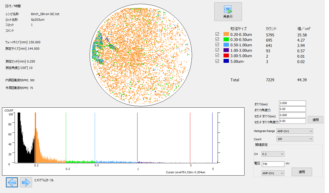
YPI-MX-DC model detects on transparent substrates, contamination of particles up to 0.1µm. Working on wafers from 2 to 8 inches, it can inspect materials such as SiC and GaN. Its laser of 355nm of wavelength eases analysis on compound semiconductor industry substrates. For the most exotic applications, it is possible to double the number of optical heads. It is also possible to add a second detector channel which improves measurement accuracy. This product is ideal for following applications:
  • Process control
  • Contamination control of wafers, including Epi on SiC and thin layers
  • Equipment contamination control
  • Polishing process control
  • Wafer reception control, coming from your suppliers
Two types of scan are available: helical or raster (XY). XY sweep allows to work on wafers and square substrates, the helical being for wafers only.

Do not hesitate to contact us to get a technical brochure by clicking here


YPI-MX-DC, specialist of surface inspection on transparent substrates

YPI-MX-DC can be equipped with two lasers of 355nm. The addition of a second optical head improves the accuracy of measurement and decreases surface effects such as roughness. This wavelength is ideal to control transparent and translucent substrates even those with thin layers. Furthermore, the equipment is able to distinguish the front face of the back face of the wafer with an edge exclusion of 3mm.
YPI-MX-DC is equipped with a standard loading port and a handling robot cassette to cassette. We propose to add in option, a second loading port as well as a double hand robot.
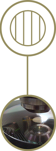
An optical microscope in option is also available. With it, you can visualize particles previously detected during inspection. A color camera of 4 mega pixels offers an image easily exportable and processable remotely directly from your desktop. 20x and 50x mag make visible particles up to 0.1µm. Moreover, a more advanced option is available to make interactive the particles map. A single click on the selected area will display it on the screen.

Do not hesitate to contact us to get a technical brochure by clicking here
 

YPI-MX for semiconductor industries

Particle inspection for transparent and opaque substrates

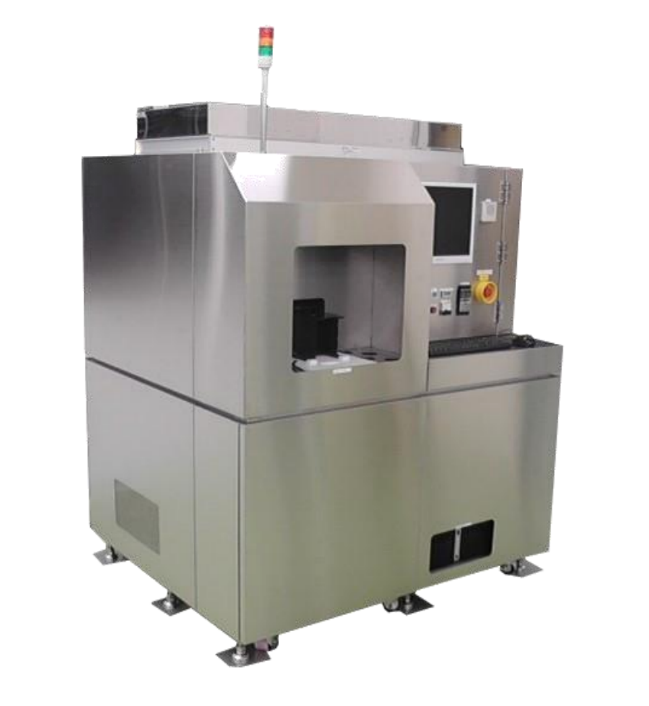
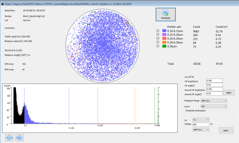
YPI-MX model can detect contamination of particles up to 0.1µm on a great variety of substrates up to 8 inches. It performs measures on Si, Crystal, Saphire, LiNb03 or LiTa03 thanks to its 405nm laser. It is possible to add a second optical head to improve measurement accuracy. Applications for this tool are wide:
  • Process control
  • Wafer contamination control, including EPI and SiC wafers and thin layers
  • Equipment contamination control
  • Polishing process control
  • Wafer reception control, coming from your suppliers

YPI-MX has another advantage. It can perform two types of scan: raster (XY) or helical sweeps. We recommend to use XY sweep for wafers and square substrate, the helical one being only for wafers.

Do not hesitate to contact us to get a technical brochure by clicking here


YPI-MX, a versatile and customizable equipment

The two lasers offer a better measurement accuracy but also reduce surface effect such as roughness. This technology detects particle up to 0.1µm. Standard edge exclusion is 3mm. The equipment is designed for both standard and specific applications.
The tool has a standard loading port as well as an automatic handling robot. This robot can charge wafers from 50mm to 200mm. In option, you can add loading ports and install a double hand robot.
It is also possible to embed an optical microscope to manually visualize particles. 20x and 50x mag allows to observe particles of respectively 3µm and 1µm. The camera transcribes in color, an image of 4 million of pixels. Furthermore, we offer an automatized particle follow-up option. It gives an interactive map to select and visualize particles thanks to the optical microscope. Save and analyze results directly from your office.

Do not hesitate to contact us to get a technical brochure by clicking here