Metrology support company for a nanoworld
Optical metrology system & support company at your service
ProductsAutomated CD and Overlay measurementUnpatterned wafer default inspectionPhotoluminescense, Thickness and Bow measurementThin filmMaterial characterization
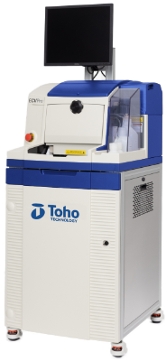
ECV Pro +
Advanced Electrochemical Capacitance Voltage
The patent-pending ECV Pro + is the result of a total redesign that completely redefines ECV profiling. We have taken 25 years of ECV profiling experience and coupled it with 25 years of advances in instrument control technology to produce the most precise, most reproducible, most highly-automated electrochemical CV profiler ever. The ECV Pro + was designed, from the ground up, to eliminate all operator dependent variations in the data. All the operator has to do is set the wafer on the stage. After initial setup, the ECV Pro + takes care of everything else.
Applications
ECV Pro introduces the first ever in-situ camera for unprecedented levels of control, ECVision™. allowing real-time imaging of the semiconductor/ electrolyte interface. Now you can see exactly what occurs at the sample surface during a measurement. For III-Nitrides, the ECV Pro GaN option extends the performance of the system for optimal profiling of GaN, InGaN and AlGaN. Hg Probe Alternative: The ECV Pro’s accuracy and reproducibility provide a viable, safe and environmentally friendly alternative to the Mercury probe. ECV Pro uses no Calomel reference electrode and is entirely Mercury free. The horizontal stage makes monitoring spatial distribution across a wafer simple and convenient. Using the depletion profi le mode and the ultra-repeatable contacting area, ECV Pro can accurately measure the surface doping variations across a wafer. Alternative to Hall: ECV Pro offers many advantages over Hall measurements. These include measurement of electrically activated dopants and individual structural layer information. Additionally, the ECV Pro can be applied to a wide range of materials and structures and is not limited to profi ling only on Si or suitable PN structures.
Features
Eliminate Operator Variability. Operator training time is reduced. Sample preparation is simplified and the intuitive software leads the operator through the measurement process step by step reducing the possibility of errors. Recipe-driven operation means no operator involvement when profiling complex structures. The novel design extends the sealing ring lifetime and eliminates the cost of expensive Calomel electrodes. Signal electrodes and contact sets need less frequent replacement. The floor standing designs reduces footprint by approximately a factor of two compared with other profilers. As the electrolyte and waste are contained on the unit, there is no need for an adjacent wet-bench.
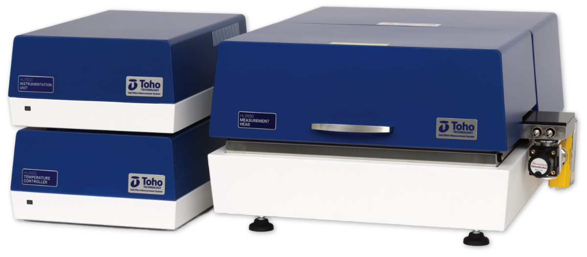
Toho HL9900
Hall effect measurement
HL9900 is a turnkey, high performance hall effect system for the measurement of resistivity, carrier concentration, and mobility in semiconductors. Modular in concept, allowing easy upgrade paths, the system is suitable for a wide variety of materials, including silicon and compound semiconductors. HL9900 has both low and high resistivity measurement capabilities. With an intuitive user interface, no programming experience is required to set up or use the HL9900.
Applications
Using Hall Effect measurement, the following properties can be determined:
• Resistivity/Conductivity • Mobility • Bulk/Sheet carrier concentration • Doping type • Hall coefficient • Magnetoresistance • Vertical/Horizontal ratio of resistance
Features
Using Hall Effect measurement, the following properties can be determined:
• Van der Pauw, Hall Bar and Bridge measurements to ASTM F-76 standard • Simple probe system for convenient, fast sample throughput • Compact bench top design • Wide current range including auto-current facility in order to minimize sample heating • User defined electric field limitation to avoid impact ionization effects at low temperatures • Optional high impedance buffer amplifier/current source to extend sheet resistivity measurements to 1011 ?/square