Automated process control by Optical Metrology
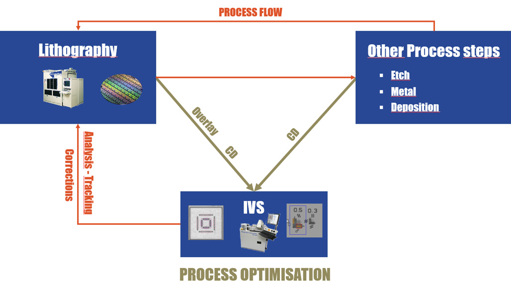
The IVS metrology can track all steps of your process and especially the photolithography steps. The key added value of the ONTO innovation IVS systems is the capability to track high volume manufacturing site and high values devices production on the different part of the process as described down below.
The IVS metrology can track all steps of your process and especially the photolithography steps. The key added value of the ONTO innovation IVS systems is the capability to track high volume manufacturing site and high values devices production on the different part of the process as described down below.
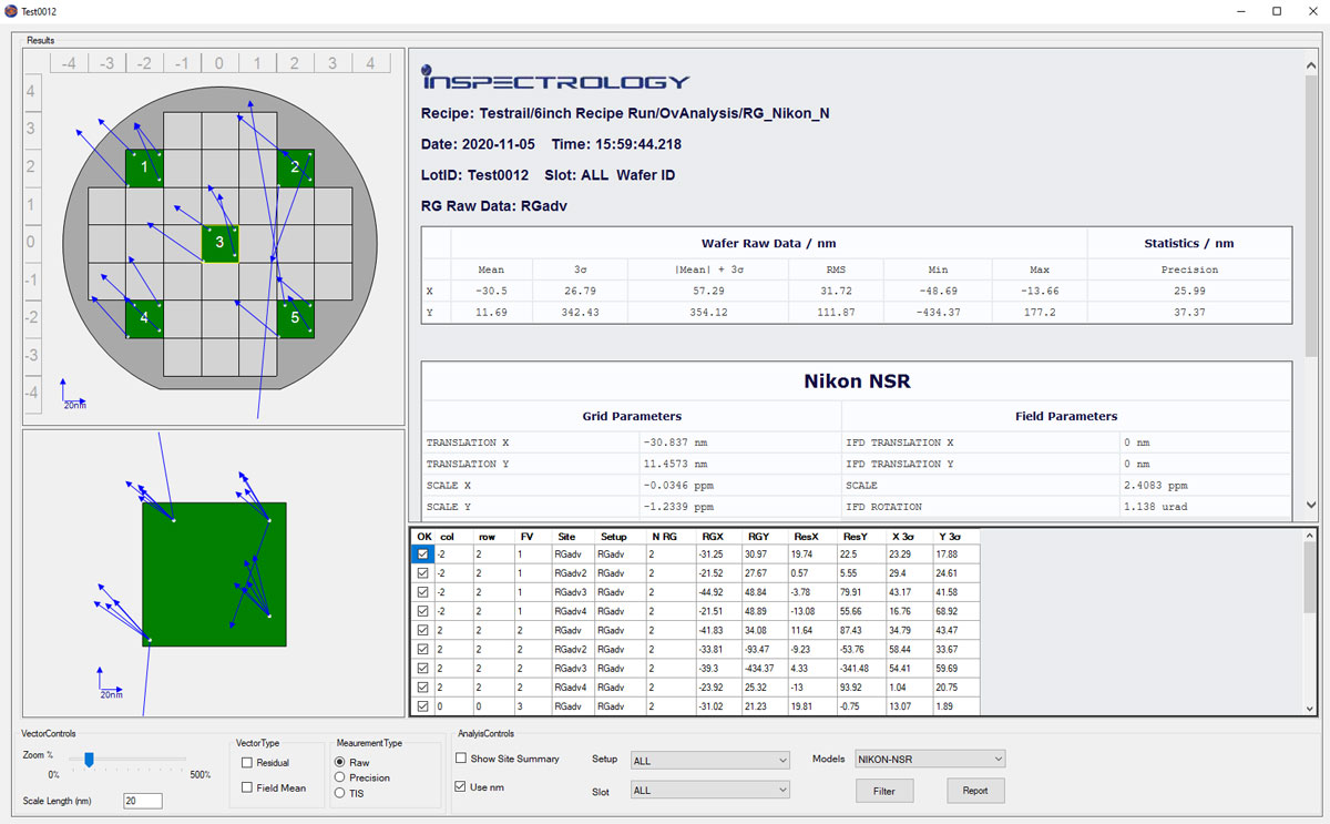
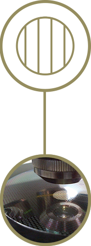
- PhotoLithography: CD / Overlay: this is the key recognize references measurement of the IVS system. High TPUT optical CD measurement and overlay registration measurement to allow photolithography engineer to achieve best process control of their process.
- Etch: CD / Overlay: In most facilities, the measurement of etched features is an essential part to certify the quality of the final products. These measurements are usually made as sampling within the production to allow the production flow to pass the threshold of the quality control.
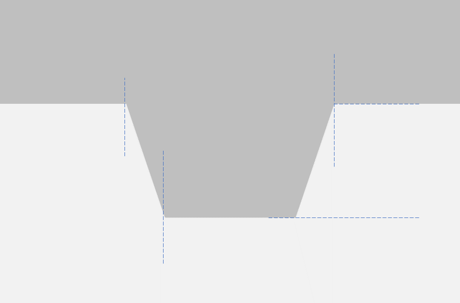
- Lift Off: CD: the new lift off processes have convey different type of measurement requirement. Within a highly populated manufacturing site, it is always recommended to have metrology tool with multiple capabilities. The IVS system is able to control the CD and the VIA at the Lift off process level as well as it can control the lithography and the etch processes.
- Film Deposition: Z Height: Within the large film deposition processes, the thickness changes are critical to the process success and to the final device’s performances. The IVS tool has the capability to measure large film thicknesses up to 120 microns thick. This metrology capacity has been particularly appreciated over the years working in the MEMS technology facilities and is now frequently used within the compound technology facility. The Z height measurement is more accurate, and 3 times faster compared to profiler metrology systems.


